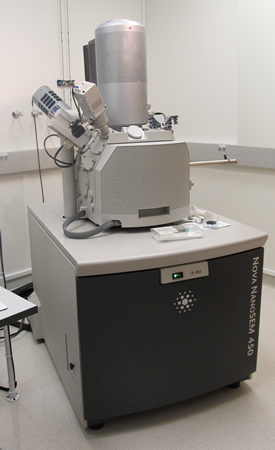
Model: Nova NanoSEM 450
Make: FEI Ltd
Description:
The Nova Nano FEG-SEM 450 is a versatile high resolution low-vacuum Field Emission Gun Scanning Electron microscope capable of producing very high resolution images of the surface of a sample. It has a wide range of applications in biological and materials science in which researchers wish to visualize and analyze the surface of a sample over a wide range of magnifications. It can be used to image over a large surface area of bulk materials as well as thin films. The FEG SEM has two modes of operation: high vacuum and low vacuum. A major feature is that it does with a single tool, what used to require multiple systems. The resolution achievable under different modes is 1-nanometers. The EDAX (with mapping system) facility provided with the instrument enables the qualitative and quantitative analysis of elements from samples.
Type of samples:
Inorganic nanomaterials, low conductive nanomaterials, nanomaterial dispersions, biological samples.
| Resolution 1.0nm at 15kV 1.4nm at 1kV 3.5nm at 100V |
Sample Navigation A 5-axes motorized x-y-z tilt-rotate stage with Eucentric tilt. Tilt +75 degrees to -15 degrees |
| Accelerating Voltage 20V to 30kV |
Beam current upto 200nA |
| Magnification X25 to X10,00,000 |
Field Emission Gun Ultra-high brightness Schottky emitter |
Applications:
Three-dimensional details of samples at very high resolution can be obtained. Examples of specimens that will be imaged include three dimensional collagenous scaffolds which are used in tissue engineering, cells adhering to and growing in tissue engineering scaffolds, nanoparticles produced by biomaterials used in hip and knee replacements, nanoparticles in body tissues and in environmental samples, fibrils of proteins that cause disease such as amyloid and prion proteins and proteins that cause muscles to contract, bacteria, virus and ultrastructural details of surface of biological samples. Detection and quantification of elements down to boron.
Model: TEAM EDS
Make: EDAX Inc, USA
| TEAM EDS Analysis system with octane SDDs deliver on the full promise of SDD technology – high speed analysis with no sacrifice in the quality of the data. |
| Silicon drift detector (SDD) provides excellent low energy performance. |
| Smart diagnostics and smart acquisition facilitate optimized collection and analysis condition. |
| Quantification for elements starting with Boron (B). |
| Elemental mapping with supporting phase data. |
| Maximum energy resolution of 129eV. |
| Measured according to ISO 15632. |
| This system is useful to academic and leading industries in the semiconductor, metals, geological, pharmaceutical, bio-materials, ceramics, etc. |
| Quantitative analysis at mapping speeds up to 200,000 cps. |